The expanding toolbox of two-dimensional (2D) materials has allowed researchers to assemble new materials that can have a disruptive impact on opto-electronic technologies. Graphene, the all-carbon 2D material, is an excellent conductor when supported on a substrate and thereby promises to be an ideal electrode material in a 2D device
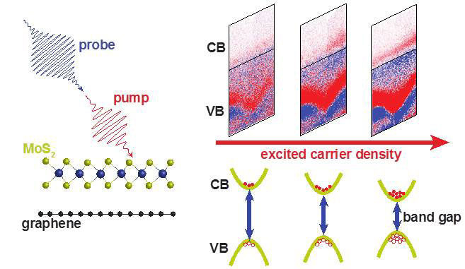
By placing a single-layer of the semiconductor molybdenum disulphide (MoS2) on top of the graphene one obtains a ‘heterostructure’ with enhanced optical properties. MoS2 plays an important role in such an assembly because it transforms from an indirect to a direct band gap semiconductor in the 2D limit. This greatly enhances the material’s ability to absorb light and leads to new properties such as an ability to discriminate the polarization of an optical excitation.
In a recent experiment performed at the Artemis facility, a team of researchers used the time- and angle-resolved photoemission spectroscopy (TR-ARPES) technique to record ultrafast snapshots of how such a 2D MoS2-graphene heterostructure responds to an optical excitation by a tuneable laser pump pulse.
Surprisingly, the band structure of the MoS2 layer changes dramatically once free carriers are excited in the valence and conduction bands of the material. The direct band gap shrinks as the number of free carriers is increased due to build-up of screening in the system. The number of free carriers and the following band gap renormalization could be controlled by the power of the pump pulse in the experiment.
Since the size of the band gap in a semiconductor determines its electronic and optical properties, the optical tuneability discovered in the MoS2-graphene heterostructure in the experiment could open new avenues for the application of 2D optoelectronic devices.